Wafer Marking Studio
Wafer Marking Studio is the all-in-one suite for SEMI-compliant laser scribing on silicon wafer back surfaces, engineered for maximum yield and 100% traceability. It features 4X density (20x36 matrix), full SEMI compliance (T7, M12, M13, T1, M1.15), auto-checksum, hardware-ready GCode export, and intuitive drag-and-drop UI.
The 4X density delivers superior contrast, resilience through backside grinding, safety with lower laser power, and durability against chemical etching. In automated fabs, Wafer Marking Studio acts as Line-Stop Insurance—preventing costly "No-Read" failures, enabling high-margin contracts with T7 Reed-Solomon error correction, and fitting within shrinking keep-out zones. Supported standards include SEMI T7, M12/M13, T1, and M1.15.
Keywords
Wafer Marking Studio
The professional all-in-one suite for SEMI-compliant laser scribing. Engineered for maximum yield and 100% traceability.
- ✅ 4X Density Native Support: Best-in-class 20x36 matrix.
- ✅ Full SEMI Compliance: T7, M12, M13, T1, and M1.15.
- ✅ Auto-Checksum: Instant verification for M12/M13.
- ✅ Hardware Ready: Export GCode or print via USB.
- ✅ Dynamic Alignment: Auto-position OCR relative to T7.
- ✅ Intuitive UI: Drag-and-drop design interface.
Get Started
Compatible with 64-bit Windows Environments

Download Demo Version
Resources, Documentation and Enterprise Licensing
Upgrade to Full Version
We offer flexible licensing models tailored to your equipment volume and facility requirements.
Why High-Density (4X) Marking Matters
Back-surface marking is difficult. Standard 5x9 fonts often fail during processing. Here is how Wafer Marking Studio solves it:
Contrast
20x36 overlap creates a solid stroke that "pops" on rough unpolished surfaces for AOI systems.
Resilience
Survives aggressive backside grinding for 3D IC/HBM stacking where 1x fonts are ground away.
Safety
Uses lower laser power with higher pulse overlap to minimize Heat Affected Zones (HAZ).
Durability
Higher surface area ensures characters remain legible even after harsh chemical wet-etch baths.
Comparison of Density Specs
| Density Type | Matrix Size | Best Use Case |
|---|---|---|
| Single (1x) | 5 x 9 |
Polished front surfaces; simple identification. |
| Double (2x) | 10 x 18 |
Standard traceability; general manufacturing purpose. |
| Triple (3x) | 15 x 27 |
Rough back surfaces; medium-grit finishes. |
| Quadruple (4x) | 20 x 36 |
Ultra-thin wafers; backside grinding; high-speed AOI reliability. |
The "Must" Reason: Eliminating the Blind Spot in Automated Fabs
In a modern "Dark" Fab, if a scanner cannot read a wafer, the entire line stops. Wafer Marking Studio isn't just a font tool—it is Line-Stop Insurance.
1. Preventing the "Ghost Wafer" Crisis
A line stop in a 300mm fab costs thousands of dollars per minute. Standard 1x fonts act as a single point of failure when backsurface noise increases.
The Must: Our Studio ensures zero-touch automation. By utilizing 4x density and T7 Data Matrix, your system never loses track of a unit, avoiding costly manual overrides.
2. Automotive & Medical Traceability
For EV (IATF 16949), Aerospace, or Medical sectors, "best effort" marking is a legal liability.
The Must: These sectors require 100% Error-Corrected traceability. T7 Data Matrix with Reed-Solomon correction is a requirement for bidding on high-margin contracts where OCR fonts are too easily corrupted.
3. The Physical Geometry Constraint
Modern wafers have shrinking "Keep-out" zones. 1x and 2x fonts are physically too large for many new designs.
The Must: To fit 18+ characters in a margin without interfering with active die areas, 4x density or T7 formats are a mathematical necessity, not a choice.
| Production Scenario | Standard SEMI Font (Optional) | Wafer Marking Studio (Required) |
|---|---|---|
| Backside Grinding | Mark becomes unreadable noise. | T7 recovers data through damage. |
| High-Margin Audits | Risk of audit failure & contract loss. | Guaranteed IATF Compliance. |
| Edge-Zone Limits | Font overlaps into active die area. | 4x Density stays within margin. |
| Line Efficiency | High "No-Read" rate causes stops. | Zero-Touch Automation Flow. |
"If your scanner can't read it, your robot won't move it."
Wafer Marking Studio: Because a 'No-Read' is a 'No-Go'.
Implementation Guides
Adding High-Density SEMI OCR Fonts
Effortlessly switch between densities to match your substrate texture.
 1x (5x9)
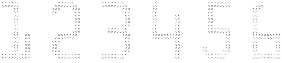 2x (10x18)
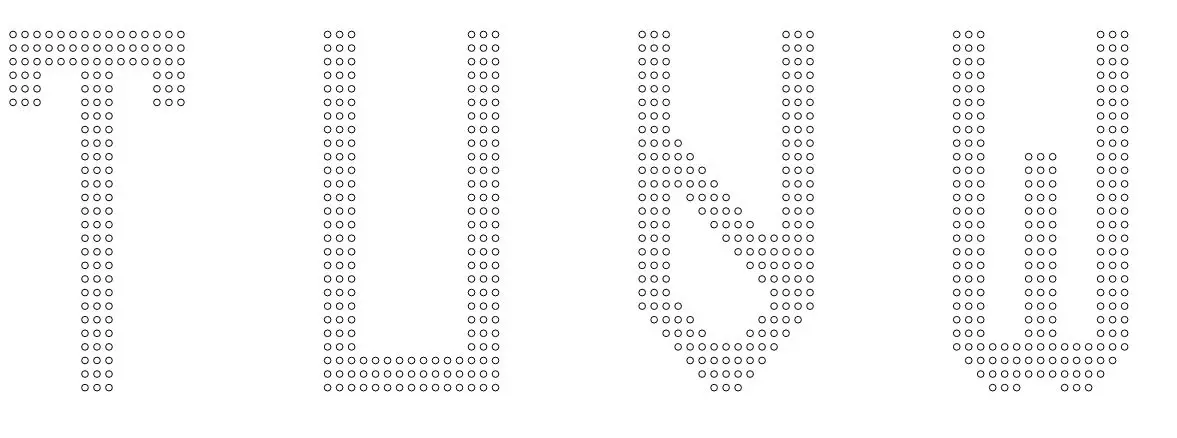 3x (15x27)
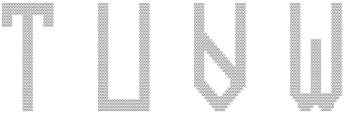 4x (20x36)
SEMI T7 Data Matrix
Supports square or circle cells. Automatically positions in the Edge Exclusive Area per SEMI standards.
SEMI T1 BC-412 Code
Native BC-412 generation for silicon wafer back-surface marking using dots or bars.
What Are Silicon Wafers?
Silicon wafers are ultra-pure crystalline slices used as the substrate for integrated circuits (ICs). Their surface quality and precise marking are vital for the microelectronics manufacturing chain.
Global Marking Standards
- SEMI T7: 2D Data Matrix for double-side polished wafers.
- SEMI M12 / M13: Alphanumeric marking protocols.
- SEMI T1: Standards for BC-412 barcode marking.
- SEMI M1.15: 300mm wafer notch & OCR/T7 alignment rules.